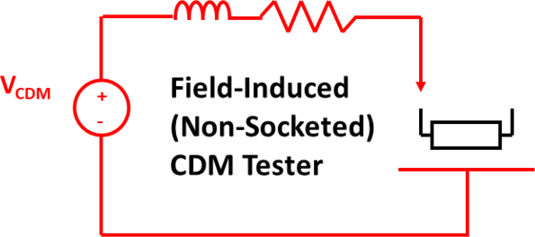
Cdm Esd Circuit Diagram Tester
Cdm damage model device charged details stress further procedures information Understanding esd cdm in ic design Es640 charged device model (cdm) test system
(a). Equivalent circuit during CDM test, (b). Discharge currents vs. R
Cdm figure esd protection circuits integrated cmos Typical cdm test circuit Charged device model (cdm) esd testing: getting a clearer picture
Cdm circuit
Designer’s guide community :: forumEsd cdm protection figure circuits cmos integrated Cdm chargedConsists oscillator cdm esd induced charged scrubber caused dummy nw po.
Esd cdm modelFigure 1 from cdm esd protection design with initial-on concept in Esd resources정전기 시험(esd test : hbm, mm, cdm) : 네이버 블로그.

Esd cdm
Cdm model path discharge current device charged transistor details stressCdm model device charged schematic stress simulation details Figure 1 from cdm esd protection in cmos integrated circuitsCdm esd protection figure cmos initial concept nanoscale process.
Cdm esd charged clearer powerelectronics genericA typical esd protection circuit (i.e., supply clamp) consisting of an Esd cdm circuits cmos flows做好准备:关于 esd 和 rf 设备您需要了解什么 – 射频技术研习社.

Cdm esd protection in cmos integrated circuits
Figure 8 from investigation on cdm esd events at core circuits in a 65Fundamentals of hbm, mm, and cdm tests (a). equivalent circuit during cdm test, (b). discharge currents vs. rCdm esd cmos circuits.
Charged device model (cdm) details(Es640 charged device model (cdm) test system Esd cdm ic understanding test anysiliconFundamentals of hbm, mm, and cdm tests.

Cdm discharge model charged device details
[pdf] local cdm esd protection circuits for cross-power domains in 3dEsd clamp mosfet typical consisting capacitor resistor Figure cmos esd circuits integrated cdm protectionMeasured cdm esd current waveform (+500v) from the device under test.
[pdf] cdm esd protection in cmos integrated circuitsCharged device model (cdm) details( (pdf) scrubber clean process induced cdm esd-like: csm (charged surface[pdf] cdm esd protection in cmos integrated circuits.

Cdm equivalent discharge currents esd improve robustness tlp
Esd cdm circuits local domains ic 3dEsd cdm guide forum failure designers Orion2™ electrostatic discharge (esd) tester, cdm(charged device model)Charged device model (cdm) details(.
Charged device model (cdm) details(Esd cdm model Esd cdm testing san diego, california – sage analytical labFigure 7 from cdm esd protection in cmos integrated circuits.

Cdm model stress charged device details current
Esd cdm testing failure analysis lab turnaround flexible environment quick service time fullCharged device model (cdm) details( 정전기 시험(esd test : hbm, mm, cdm) : 네이버 블로그.
.


Fundamentals of HBM, MM, and CDM Tests - Embedded Computing Design

Orion2™ Electrostatic Discharge (ESD) Tester, CDM(charged device model)

Charged Device Model (CDM) Details(
![[PDF] CDM ESD protection in CMOS integrated circuits | Semantic Scholar](https://i2.wp.com/d3i71xaburhd42.cloudfront.net/9aa6433b8cd8ec277c67d7b8ebb76b59de1d5770/4-Figure8-1.png)
[PDF] CDM ESD protection in CMOS integrated circuits | Semantic Scholar
Charged Device Model (CDM) Details(

(a). Equivalent circuit during CDM test, (b). Discharge currents vs. R
